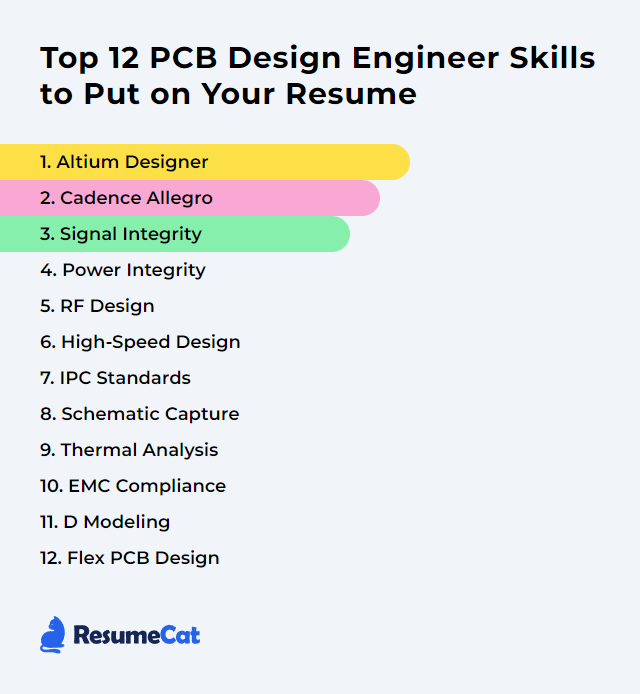
Top 12 PCB Design Engineer Skills to Put on Your Resume
In today’s crowded job market, a PCB Design Engineer’s resume needs to pulse with hard technical skill, practical creativity, and the grit to solve messy problems. Spotlighting the right capabilities signals confidence, cuts through noise, and opens doors in the fast-shifting world of electronics design.
PCB Design Engineer Skills
- Altium Designer
- Cadence Allegro
- Signal Integrity
- Power Integrity
- RF Design
- High-Speed Design
- IPC Standards
- Schematic Capture
- Thermal Analysis
- EMC Compliance
- 3D Modeling
- Flex PCB Design
1. Altium Designer
Altium Designer is a unified PCB design platform with schematic capture, layout, rules-driven DRC, and 3D visualization, making complex multilayer boards easier to plan, execute, and verify.
Why It's Important
It streamlines the full design flow—from schematics to layout to outputs—so you move faster, catch errors earlier, and ship cleaner designs with fewer surprises.
How to Improve Altium Designer Skills
Grow depth, not just clicks. A quick path:
Nail the fundamentals: Work through a complete schematic-to-layout workflow until it’s muscle memory.
Push advanced features: Constraints, design rules, interactive routing, variants, managed libraries—use them daily.
Study real projects: Rebuild existing boards, then rework and optimize them. Shorten routes. Tighten clearances. Tame the PDN.
Tune your workspace: Custom shortcuts, panels, templates, output jobs. The right setup saves hours.
Stay current: Track release notes; fold new features into your process early.
Learn from peers: Forums, webinars, and expert talks are gold for obscure tricks and gotchas.
Habit beats hacks. Build, review, repeat.
How to Display Altium Designer Skills on Your Resume
2. Cadence Allegro
Cadence Allegro (Allegro PCB Designer) is a robust suite for complex multilayer boards with strong routing, constraint management, and manufacturing handoff capabilities.
Why It's Important
It handles high-speed, high-density designs with rigorous rules and analysis, helping you build boards that meet performance and production realities.
How to Improve Cadence Allegro Skills
Start with official docs and training: Learn the core workflows and what’s new each release.
Practice on tough boards: Differential pairs, length tuning, blind/buried vias, dense BGA escapes—chase the hard problems.
Automate: Use scripts and SKILL where it helps. Little automations add up.
Customize constraints: Build reusable, product-specific constraint sets that reflect your stackups and processes.
Engage communities: Q&A, tips, user groups—learn from real-world edge cases.
Learn shortcuts: Speed matters. Reduce clicks. Keep your hands on the keyboard.
Consistency and constraint discipline will sharpen outcomes and cycle times.
How to Display Cadence Allegro Skills on Your Resume
3. Signal Integrity
Signal integrity is the art and science of keeping waveforms faithful from driver to receiver. Clean edges, controlled impedance, low noise. No surprises in timing or eye diagrams.
Why It's Important
Poor SI sinks products: data errors, flaky links, radiated emissions, field failures. Good SI makes speed reliable and repeatable.
How to Improve Signal Integrity Skills
Route with intent: Control impedance. Keep reference planes continuous. Avoid stubs and excessive vias on fast nets.
Manage return paths: Give high-speed currents a tight, uninterrupted return. Stitch grounds near layer transitions.
Use terminations smartly: Series, parallel, or AC terminations where they make sense to tame reflections and ringing.
Design the PDN: Solid planes, short paths, and targeted decoupling keep supply noise from corrupting signals.
Differential pairs: Match impedance, length, and coupling. Control skew. Keep pairs over solid reference planes.
Layer stack discipline: Place high-speed layers adjacent to ground. Choose dielectrics for controlled impedance and loss.
Simulate early: Pre- and post-layout SI checks catch the gremlins before they reach the lab.
How to Display Signal Integrity Skills on Your Resume

4. Power Integrity
Power integrity ensures every component sees a stable, clean supply across load steps and frequency. A quiet, low-impedance PDN keeps systems honest.
Why It's Important
Unstable rails trigger timing jitter, bit errors, resets, and heat. Solid PI fortifies performance and lifespan.
How to Improve Power Integrity Skills
Architect the PDN: Model target impedance. Plan planes, shapes, and vias to keep it low where it counts.
Place decoupling with purpose: Close to pins, right values, right ESL/ESR mix. Use multiple capacitance ranges.
Tight plane coupling: Thin dielectrics between power and ground reduce inductance and spread current.
Size power traces correctly: Calculate width for current, temperature rise, and drop. Keep critical paths short and direct.
Simulate: Use PI tools (e.g., Sigrity, ADS) early to predict resonances and hot spots.
Measure: Validate with scopes and probes. Correlate lab results with models and iterate.
How to Display Power Integrity Skills on Your Resume

5. RF Design
RF design covers circuits that transmit or receive radio frequencies from roughly 3 kHz to 300 GHz. Layout, matching, isolation, grounding, materials—every choice nudges performance.
Why It's Important
Wireless lives or dies on RF behavior. Interference, loss, and detuning wreck range and throughput. Good RF design dodges those traps.
How to Improve RF Design Skills
Place with intent: Short RF paths. Keep digital noise away. Orient components to simplify matching and filtering.
Impedance matching: Use microstrip/stripline with controlled impedance. Tune with stubs, L, or Pi networks.
Stackup first: Lock dielectric, copper thickness, and reference planes to protect loss and impedance.
Ground like you mean it: Continuous ground under RF traces. Stitch vias to fence and contain fields.
Decouple and filter: Tight decoupling at RF ICs. Use SAW/BAW filters or LC sections to clean up harmonics and noise.
Shield and isolate: Partition RF from digital. Use cans or keep-outs where needed.
Pick the right material: Low-loss dielectrics and stable Dk reduce detuning and insertion loss at frequency.
Simulate and verify: EM and circuit sims guide the layout. Then measure: S-parameters, return loss, radiation.
How to Display RF Design Skills on Your Resume

6. High-Speed Design
High-speed design tames reflections, crosstalk, losses, and EMI so fast signals arrive intact and on time. Precision routing meets disciplined stackups.
Why It's Important
As edges get faster, the board becomes part of the circuit. Robust high-speed practice keeps links solid and data honest.
How to Improve High-Speed Design Skills
Control impedance: Calculate and constrain it. Verify with field solvers or stackup tools.
Terminate correctly: Series or parallel as needed to squash reflections.
Fight crosstalk: Increase spacing, use orthogonal routing on adjacent layers, and add ground between aggressors and victims where practical.
Power and decoupling: Solid PDN design reduces jitter and ground bounce that pollute fast nets.
Use differential pairs: Control pair impedance, coupling, and skew. Match lengths within tight budgets.
Keep it clean: Short traces, minimal vias, route over continuous reference planes, no sharp corners on critical nets.
Mind return paths: Ensure direct, low-inductance returns. Stitch grounds near layer changes.
Simulate, then probe: SI/PI/EMI simulations first; scope and VNA work confirms behavior after.
Study continuously: Application notes, conference talks, and journals sharpen intuition.
How to Display High-Speed Design Skills on Your Resume

7. IPC Standards
IPC standards define shared expectations for design, fabrication, and assembly. They align engineers, fabricators, and assemblers on what “good” looks like.
Why It's Important
Following IPC raises reliability, eases vendor communication, and avoids guesswork during review, build, and inspection.
How to Improve IPC Standards Skills
Stay current: Track revisions for documents you rely on (e.g., IPC-A-600, IPC-6012, IPC-2221/2222/2223).
Get certified where it counts: Training cements the details you might otherwise miss.
Design to DFM/DFA: Bake requirements in early so builds flow smoothly at your vendors.
Use checklists: IPC-driven reviews catch common pitfalls before release.
Participate: Engage with standards communities and bring back best practices to your team.
How to Display IPC Standards Skills on Your Resume
8. Schematic Capture
Schematic capture turns intent into a clear, checkable circuit blueprint—symbols, nets, constraints, and the logic that ties it all together.
Why It's Important
It’s the source of truth for layout and manufacturing. Good schematics prevent ambiguity, cut errors, and speed reviews.
How to Improve Schematic Capture Skills
Build hierarchies: Break big designs into blocks. Reuse. Keep complexity contained.
Standardize libraries: Curate symbols, footprints, parameters, and 3D models. Lock naming and pin mapping.
Run DRCs early and often: Catch unconnected pins, wrong nets, duplicate references—before layout.
Cross-probe: Bounce between schematic and PCB to validate intent and fix mismatches quickly.
Version control: Branch for features and fixes. Tag releases. Document changes.
Keep learning: Courses and vendor trainings sharpen both speed and clarity.
How to Display Schematic Capture Skills on Your Resume
9. Thermal Analysis
Thermal analysis evaluates how heat forms, spreads, and escapes across your PCB so components stay within safe operating limits.
Why It's Important
Overheating erodes reliability and throttles performance. Good thermal work avoids hot spots, runaway conditions, and premature failures.
How to Improve Thermal Analysis Skills
Choose materials wisely: Consider thermal conductivity, Tg, and thickness early. Don’t let the stackup trap heat.
Place heat sources smartly: Spread them out. Keep sensitive parts away from the blast radius.
Use thermal vias: Arrays beneath hot packages pull heat into planes or attached sinks.
Heatsinks and interfaces: Pair devices with proper sinks and use quality TIMs to cut interface resistance.
Leverage planes: Wide copper pours help spread heat; tie them in with plenty of vias.
Simulate realistically: Model airflow, boundary conditions, and power profiles. Then correlate to lab data.
Plan cooling paths: Ducting, fans, vents, or just clear airflow—design the enclosure and board as a system.
How to Display Thermal Analysis Skills on Your Resume

10. EMC Compliance
EMC compliance means your product doesn’t bother others and isn’t bothered itself. Good layout lowers emissions and boosts immunity.
Why It's Important
Failing compliance costs time, money, and reputation. Passing early saves all three.
How to Improve EMC Compliance Skills
Grounding strategy: Continuous ground planes, short returns, and smart stitching reduce loop areas and noise.
Trace discipline: Short high-speed runs, differential pairs where appropriate, and careful layer transitions.
Decoupling and filtering: Localized decaps, ferrites or filters on noisy and sensitive lines, and clean I/O boundaries.
Shielding and guards: Shields for sensitive blocks. Guard traces tied to ground to protect critical nets.
Thoughtful placement: Separate noisy from quiet domains. Align fields to cancel, not reinforce.
Stackup for EMC: Signal layers sandwiched between planes to contain fields and cut emissions.
Pre-compliance testing: Probe, sniff, and scan early. Fix issues when changes are still cheap.
How to Display EMC Compliance Skills on Your Resume
11. 3D Modeling
3D modeling builds an accurate digital twin of your PCB and enclosure space. Fit, clearance, collision checks, and mechanical context come alive before metal is cut.
Why It's Important
It prevents last-minute mechanical clashes, helps with thermal and airflow planning, and smooths ECAD–MCAD collaboration.
How to Improve 3D Modeling Skills
Master your ECAD tools: Use 3D previews, mechanical layers, keepout definitions, and step-model integration routinely.
Curate 3D libraries: Verified STEP models with correct origins and heights save rework and prevent collisions.
Practice ECAD–MCAD exchange: Establish a clean workflow for STEP or incremental sync with your mechanical team.
Design for manufacturing: Respect clearances, tolerances, connector z-heights, and assembly access.
Simulate where helpful: Use mechanical checks and, when needed, thermal or structural analysis for critical areas.
Iterate with feedback: Fold fab/assembly notes and field learnings back into models and templates.
How to Display 3D Modeling Skills on Your Resume
12. Flex PCB Design
Flex PCB design creates circuits that bend, fold, and move. Materials, stackups, and routing must respect mechanical realities to survive repeated flexing.
Why It's Important
Flex unlocks small, light, and unconventional product forms. It also reduces connectors and assembly complexity—if designed with durability in mind.
How to Improve Flex PCB Design Skills
Pick the right materials: Polyimide, adhesives, and coverlays suited to the environment and bend profile.
Respect bend radius: Maintain a bend radius of at least 10× the flex thickness for dynamic bends (larger is safer).
Hatched ground in flex zones: Use hatching (not solid copper) in bend regions to boost flexibility and reduce cracking risks.
Reinforce pads and vias: Teardrops, anchors, and extra coverlay support reduce stress concentrations.
Anchor rigid components: Keep heavy or non-flex elements away from bend areas and secure them firmly.
Route with care: Uniform widths, smooth curves, and traces perpendicular to the bend where possible.
Smooth rigid–flex transitions: Provide gradual transitions and support to avoid stress at the junction.
Prototype and test: Dynamic bend tests and environmental checks expose weaknesses before volume build.
How to Display Flex PCB Design Skills on Your Resume