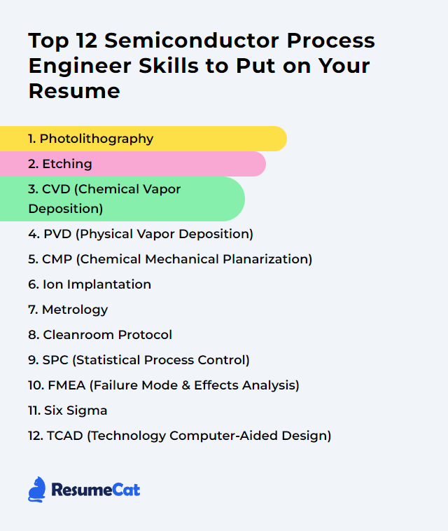
Top 12 Semiconductor Process Engineer Skills to Put on Your Resume
Semiconductor manufacturing shifts fast, and a process engineer’s toolkit decides whether ideas fly or fizzle. Make your resume whisper competence and shout clarity by showcasing the right skills—twelve core strengths that speak to yield, reliability, and speed.
Semiconductor Process Engineer Skills
- Photolithography
- Etching
- CVD (Chemical Vapor Deposition)
- PVD (Physical Vapor Deposition)
- CMP (Chemical Mechanical Planarization)
- Ion Implantation
- Metrology
- Cleanroom Protocol
- SPC (Statistical Process Control)
- FMEA (Failure Mode and Effects Analysis)
- Six Sigma
- TCAD (Technology Computer-Aided Design)
1. Photolithography
Photolithography transfers geometric patterns onto a wafer using a photoresist, exposure through a patterned mask, and development to define features for etch or deposition. This is the scalpel of chipmaking, shaping nanometer-scale structures with ruthless precision.
Why It's Important
It’s the gateway to density and speed. Precise patterning unlocks smaller transistors, tighter interconnects, and cleaner overlay—every node depends on it.
How to Improve Photolithography Skills
Better litho comes from tighter control and smarter tooling:
Resolution Enhancement: Push Immersion Lithography, Multiple Patterning, and EUV; explore High-NA EUV as it ramps for finer features.
Photoresist Optimization: Tune sensitivity, contrast, and line-edge roughness performance; track advances from industry consortia and technical conferences such as SPIE.
Exposure Control: Sharpen overlay and focus with meticulous mask alignment, stage calibration, and dose mapping.
Process Control: Use advanced process control to stabilize CDs and overlay across lots and tools.
Light Source Strategy: Match source coherence and illumination settings to pattern types; optimize source-mask settings for complex layouts.
Computational Lithography: Apply Source Mask Optimization and Inverse Lithography Technology for pattern fidelity and process window gains.
Equipment Maintenance: Calibrate stages, optics, and environmental controls on a strict schedule to keep drift and particles at bay.
Incremental gains stack. Small CD improvements today become big yield wins tomorrow.
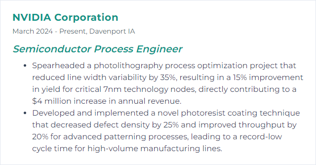
How to Display Photolithography Skills on Your Resume
2. Etching
Etching selectively removes material from wafers using wet chemistries or dry plasma processes. It sculpts features, opens vias, and defines sidewalls that must be crisp, vertical, and uniform.
Why It's Important
Transistor performance and interconnect reliability hinge on the exactness of etched features. Poor selectivity or profile control ripples into device failures and yield pain.
How to Improve Etching Skills
Dial in the physics and chemistry, then guard it with control:
Optimize Etch Parameters: Balance pressure, RF power, bias, gas ratios, and temperature for rate, selectivity, and uniformity. MicroChemicals Etching Basics.
Choose the Right Technique: Wet vs. dry, RIE vs. ICP vs. DRIE—match method to material stack, aspect ratio, and profile targets. AZoM Etching Techniques.
Advanced Masking: Use robust hard masks or multilayer stacks when polymers or resists fall short. ScienceDirect - Etching Process.
Real-Time Monitoring: Endpoint detection and chamber health checks maintain consistency lot to lot. Semiconductor Engineering - Etch.
Modeling and Simulation: CFD and feature-scale models predict ion/neutral dynamics and help preempt costly trials. CFD Online.
Relentless Learning: Track new chemistries, pulsed plasmas, and profile control methods. IEEE Xplore.
Control the chamber, control the device geometry. It’s that direct.
How to Display Etching Skills on Your Resume

3. CVD (Chemical Vapor Deposition)
CVD deposits thin films from gaseous precursors at elevated temperatures, enabling controlled composition, conformality, and thickness for dielectrics, conductors, and barrier layers.
Why It's Important
It builds the stacks. Uniform, pure, well‑adhered films underpin device performance, isolation, and reliability across massive wafer counts.
How to Improve CVD (Chemical Vapor Deposition) Skills
Improving Chemical Vapor Deposition means cleaner chemistries, tighter control, and fewer surprises:
Precursor Selection: Choose high‑purity, thermally stable precursors with appropriate volatility and reactivity. Guidance from vendors such as SAMCO is useful.
Temperature Control: Stabilize substrate and chamber temperatures to steer film stress, density, and stoichiometry. Lam Research has strong insights on temperature management.
Pressure and Flow: Tune total pressure, residence time, and gas distribution for uniform coverage. Applied Materials offers approaches to advanced flow control.
Plasma Enhancement: For PECVD, optimize power, frequency, and duty cycles to reduce damage while boosting rates. Oxford Instruments publishes practical guidance.
In‑situ Monitoring: Real‑time thickness, refractive index, or emission monitoring stabilizes outcomes. KLA’s metrology approaches are instructive.
Chamber Health: Regular cleans, seasoning, and parts life tracking suppress particles and drift. ASM highlights maintenance strategies.
Modeling and DOE: Use simulation tools and structured experiments (DOE) to converge faster. Coventor and similar platforms help derisk changes.
Small tweaks in temperature or flow can flip stress sign, shift refractive index, or unlock uniformity—measure, then move.
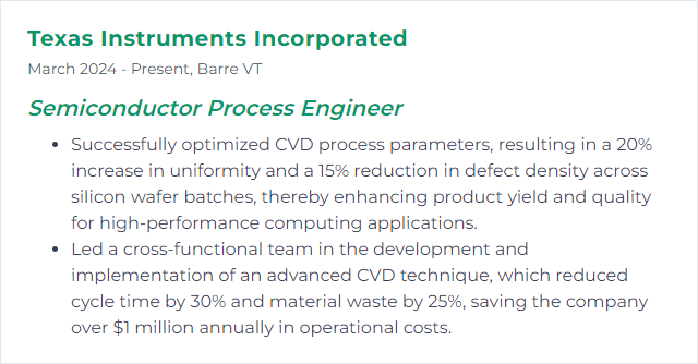
How to Display CVD (Chemical Vapor Deposition) Skills on Your Resume
4. PVD (Physical Vapor Deposition)
PVD forms thin films in vacuum via sputtering or evaporation, condensing atoms onto the wafer. Great for metals, barriers, and seed layers.
Why It's Important
Interconnects and contacts depend on clean, adherent, uniform metal films. Poor step coverage or contamination shows up later as resistive nightmares.
How to Improve PVD (Physical Vapor Deposition) Skills
Better PVD comes from beam control, target quality, and chamber discipline:
Deposition Parameters: Balance substrate temperature, pressure, target power, and geometry for uniform films and grain control. Reference: Semiconductor Engineering.
Advanced Targets: High‑purity, high‑density targets reduce particles and improve film consistency. ScienceDirect provides useful overviews.
Equipment Upgrades: Rotating fixtures, collimation, or long‑throw designs improve step coverage and uniformity. IOPscience offers technical background.
In‑situ Monitoring: Rate control, plasma diagnostics, and endpoint cues keep the process honest. MDPI has methodology reviews.
New Techniques: Evaluate HiPIMS for dense films and improved adhesion without big thermal budgets. Elsevier has broad surveys.
Keep targets clean, shields fresh, and wafers grounded—film quality follows.
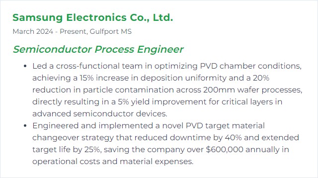
How to Display PVD (Physical Vapor Deposition) Skills on Your Resume
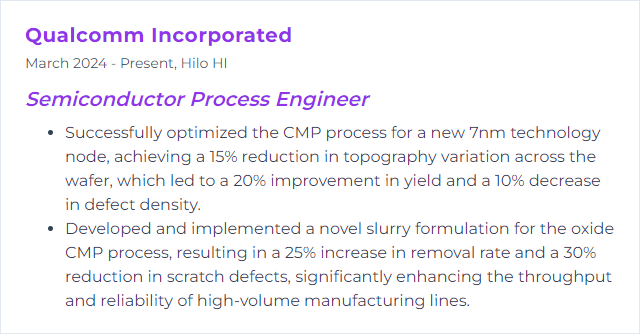
5. CMP (Chemical Mechanical Planarization)
CMP combines chemical slurry with mechanical polishing to flatten wafer surfaces, enabling tight depth-of-focus windows and clean interlayer stacking.
Why It's Important
Planarity makes lithography possible and interconnects behave. Without CMP, layers wander and patterns blur.
How to Improve CMP (Chemical Mechanical Planarization) Skills
Control the consumables, then the kinematics:
Slurry Optimization: Tune abrasive size, oxidizers, complexing agents, and pH for removal rate and selectivity. Slurry Optimization.
Pad Conditioning: Maintain pad asperity with the right conditioners and schedules to prevent glazing. Pad Conditioning Effects.
Process Parameters: Balance pressure, relative velocity, and temperature to curb defects and dishing. Process Parameters Influence.
Post‑CMP Clean: Remove residues and particles with chemistry and megasonics tuned to the material stack. Post‑CMP Cleaning.
Better uniformity upstream means fewer headaches downstream.
How to Display CMP (Chemical Mechanical Planarization) Skills on Your Resume
6. Ion Implantation
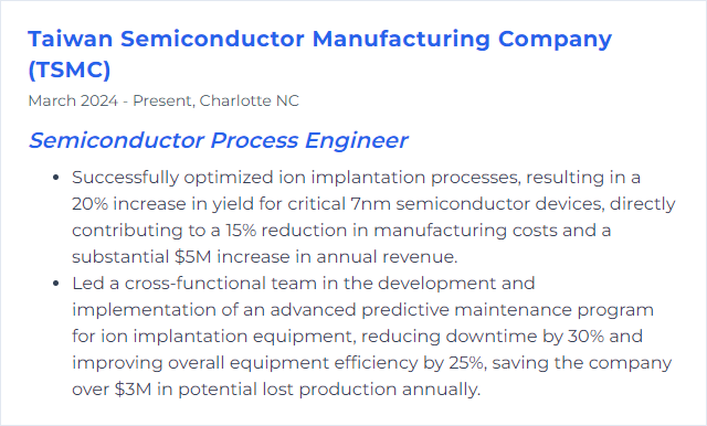
Ion implantation drives dopant ions into the wafer with controlled energy and dose, setting junction depths and concentrations with surgical accuracy.
Why It's Important
Doping profiles define device thresholds, leakage, and speed. Precision here echoes through the whole transistor stack.
How to Improve Ion Implantation Skills
Keep the beam steady, the dose honest, and the damage healed:
Dose and Energy Control: Use simulation tools to predict profiles and tune energy/dose to spec.
Implanter Health: Routine calibration and maintenance stabilize beam current, energy spread, and scan uniformity.
Advanced Methods: Consider cluster ions or PIII for better conformity and lower damage in tricky topographies.
Process Monitoring: Real‑time beam diagnostics and endpoint signals help catch drift early.
Damage Recovery: Post‑implant anneal—spike, laser, or flash—activates dopants and repairs lattice disruptions.
Profile accuracy plus smart annealing equals predictable devices.
How to Display Ion Implantation Skills on Your Resume
7. Metrology
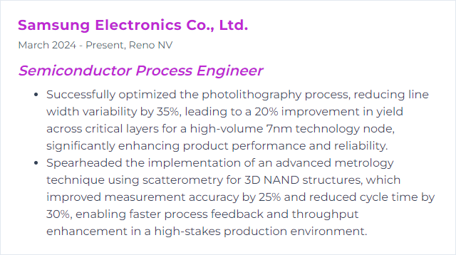
Metrology is the measurement backbone—dimensions, thicknesses, composition, roughness, overlay—all quantified with repeatable rigor.
Why It's Important
What you can’t measure, you can’t control. Yield climbs when measurements are precise, trusted, and real‑time enough to steer processes.
How to Improve Metrology Skills
Sharper tools, stronger methods, steadier results:
Advanced Tooling: Atomic force microscopy, ellipsometry/scatterometry, XRR, CD‑SEM—pick the right instrument for the feature scale.
Regular Calibration: Tie tools to traceable standards and keep calibration cycles tight. NIST guidance is a good anchor.
SPC Integration: Feed metrology data into SPC to spot drift early; analyze with platforms like MINITAB.
Training: Keep operators and engineers current on methods and uncertainty analysis; SEMI programs are helpful.
Expert Collaboration: Engage with industry groups and technical societies such as IEEE to exchange practices.
Procedure Discipline: Standardize sampling, site locations, and recipes to shrink measurement variation.
Machine Learning: Apply models for outlier detection, tool health prediction, and virtual metrology.
Good metrology is quiet and relentless—always watching, rarely failing.
How to Display Metrology Skills on Your Resume
8. Cleanroom Protocol
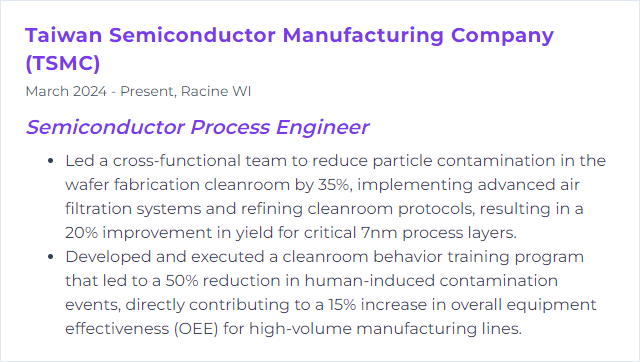
Cleanroom protocol governs garments, behavior, materials flow, and equipment care to keep particles, ions, and organics ruthlessly low.
Why It's Important
Contamination kills yield. Protocol keeps wafers pristine enough for nanoscale features to survive fabrication.
How to Improve Cleanroom Protocol Skills
Habits and systems—build both:
Regular Training: Ongoing training on gowning, handling, and incident response to keep standards fresh.
Dress Code Enforcement: No shortcuts—proper garments, correct donning sequence, and strict zone compliance.
Equipment Maintenance: Scheduled PMs reduce unexpected particle bursts or leaks.
Air Filtration: Maintain and test HEPA/ULPA filters; monitor airflow and pressure differentials.
Contamination Control: Tight protocols for material ingress/egress, approved wipes and solvents, and regular surface audits.
Process Optimization: Reduce open handling and unnecessary steps; close lids, shorten travel, simplify flows.
Audits: Frequent audits to catch creeping bad habits.
Monitoring Tech: Real‑time particle and AMC monitors to catch issues before wafers do.
Culture matters. Clean work is learned, then enforced.
How to Display Cleanroom Protocol Skills on Your Resume
9. SPC (Statistical Process Control)
SPC uses statistics to watch processes in real time—separating noise from signal and guiding corrections before defects erupt.
Why It's Important
It’s the early-warning system. Better control charts, smarter alarms, fewer excursions, more yield.
How to Improve SPC (Statistical Process Control) Skills
Make the data clean, the models smart, the actions quick:
Data Collection: High‑quality, time‑synced signals from tools and sensors; modern acquisition methods discussed widely by Semiconductor Engineering.
Advanced Software: Use platforms with real‑time analytics, multivariate capability, and alerting; enterprise solutions from vendors such as Siemens fit well.
Staff Education: Teach SPC concepts, chart selection, and interpretation; ASQ programs are solid.
Multivariate Analysis: Move beyond univariate charts to catch correlated drifts. Journal of Quality Technology has strong references.
Machine Learning: Predict excursions and recommend setpoint nudges using tools like TensorFlow ecosystems.
Continuous Improvement Culture: Let SPC findings drive Kaizen. Lean Manufacturing Tools provides practical frameworks.
Periodic Strategy Reviews: Update control plans as tools, nodes, and targets evolve.
SPC only works if people listen—and act.
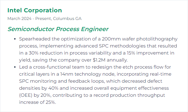
How to Display SPC (Statistical Process Control) Skills on Your Resume
10. FMEA (Failure Mode and Effects Analysis)
FMEA systematically lists how a process can fail, estimates risk, and prioritizes fixes before problems hit production.
Why It's Important
It hardens processes. You catch weak points early, protect yield, and build reliability into the flow.
How to Improve FMEA (Failure Mode and Effects Analysis) Skills
Make it collaborative, current, and action‑oriented:
Cross‑Functional Teams: Pull in design, equipment, process, quality, and maintenance for full coverage; ASQ guidance is helpful.
Use Current Data: Leverage latest SPC trends, excursion logs, and tool histories; align with SEMI standards where applicable.
Risk Prioritization: Apply RPN or modern severity‑occurrence‑detection methods with clear thresholds; IEEE Xplore has perspectives on optimization.
Continuous Learning: Roll in lessons learned from NCMRs and near‑misses; Semiconductor Industry Association resources add context.
Integrate Quality Tools: Link FMEA to SPC, control plans, and Root Cause Analysis; NIST’s Engineering Statistics Handbook is a strong primer.
Regular Refresh: Update FMEAs for new materials, recipes, or equipment; Journal of Quality in Maintenance Engineering shares practical cases.
Preventive Focus: Spend more energy preventing than correcting; Lean Enterprise Institute principles apply.
FMEA is alive only if it changes when your fab does.
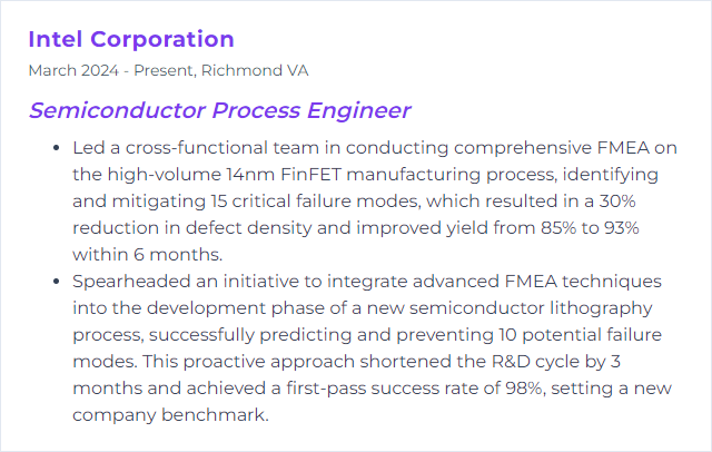
How to Display FMEA (Failure Mode and Effects Analysis) Skills on Your Resume
11. Six Sigma
Six Sigma blends statistics, structure, and discipline to crush variation and defects through DMAIC and data‑driven decisions.
Why It's Important
Semiconductor processes are complex and unforgiving. Six Sigma keeps them tight, repeatable, and economical.
How to Improve Six Sigma Skills
Push practice over buzzwords:
Solid Foundations: Master the core methods and vocabulary; ASQ materials are dependable.
Data First: Collect process‑specific data and analyze with statistical software like Minitab.
Ongoing Training: Pursue Lean Six Sigma Green/Black Belt certifications to deepen tools and tactics.
Cross‑Functional Work: Build teams that span process, equipment, and quality; collaboration tools help keep momentum.
DMAIC Rigor: Define cleanly, measure relentlessly, analyze causally, improve pragmatically, control visibly; SIA case studies offer context.
Benchmarking: Compare against industry metrics and research via IEEE Xplore and similar sources.
Voice of Customer: Feed back field performance and reliability data through structured surveys and returns analysis.
Stay Current: Track new methods and apply them where they make sense; Semiconductor Engineering is a useful channel.
Results beat rituals. Let the data steer every step.
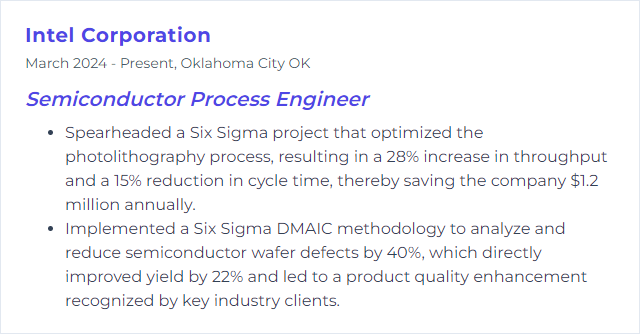
How to Display Six Sigma Skills on Your Resume
12. TCAD (Technology Computer-Aided Design)
TCAD simulates processes and devices before you cut a single wafer, shortening development loops and reducing risk.
Why It's Important
Accurate simulations mean fewer blind experiments, faster learning, and smarter tradeoffs between performance, power, and cost.
How to Improve TCAD (Technology Computer-Aided Design) Skills
Elevate fidelity and speed, then scale up:
Modern Toolsets: Keep software current; platforms such as Synopsys TCAD and Silvaco TCAD offer robust solvers and models.
Model Accuracy: Calibrate with experimental data—profiles, IV curves, CV, TEM—to ground simulations in reality.
Compute Efficiency: Use HPC or cloud resources to slash runtimes for large parametric sweeps.
Skill Growth: Follow vendor webinars, courses, and university programs to sharpen methods.
Community and Collaboration: Engage with research groups and professional networks for tips, scripts, and validation strategies.
Automation and Integration: Script workflows, link to SPICE/PDK flows, and tie results into design verification.
Simulate broadly, validate tightly, iterate quickly.
How to Display TCAD (Technology Computer-Aided Design) Skills on Your Resume

